MEMS (Micro Electro-Mechanical Systems) Technology
In less than 20 years, MEMS (micro electro-mechanical systems) technology has gone from an interesting academic exercise to an integral part of many common products. But as with most new technologies, the practical implementation of MEMS technology has taken a while to happen. The design challenges involved in designing a successful MEMS product (the ADXL2O2E) are described in this article by Harvey Weinberg from Analog Devices.
In early MEMS systems a multi-chip approach with the sensing element (MEMS structure) on one chip, and the signal conditioning electronics on another chip was used. While this approach is simpler from a process standpoint, it has many disadvantages:
* The overall silicon area is generally larger.
* Multi chip modules require additional assembly steps.
* Yield is generally lower for multi chip modules.
* Larger signals from the sensor are required to overcome the stray capacitance of the chip to chip interconnections, and stray fields necessitating a larger sensor structure.
* Larger packages are generally required to house the two-chip structure.
Of course, history teaches us that integration is the most cost effective and high performance solution. So Analog Devices pursued an integrated approach to MEMS where the sensor and signal conditioning electronics are on one chip.
Figure 1
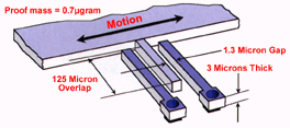
The latest generation ADXL2O2E is the result of almost a decades worth of experience building integrated MEMS accelerometers. It is the world's smallest mass-produced, low g, low cost, integrated MEMS dual axis accelerometer.
The mechanical structure of the ADXL2O2E is shown in Figure 1 along with some key dimensions in Figure 2.
Figure 2
Polysilicon springs suspend the MEMS structure above the substrate such that the body of the sensor (also known as the proof mass) can move in the X and Y axes. Acceleration causes deflection of the proof mass from its centre position. Around the four sides of the square proof mass are 32 sets of radial fingers.
These fingers are positioned between plates that are fixed to the substrate. Each finger and pair of fixed plates make up a differential capacitor, and the deflection of the proof mass is determined by measuring the differential capacitance.
This sensing method has the ability of sensing both dynamic acceleration (i.e. shock or vibration) and static acceleration (i.e. inclination or gravity).The differential capacitance is measured using synchronous modulation/demodulation techniques. After amplification, the X and Y axis acceleration signals each go through a 32KOhm resistor to an output pin (Cx and Cy) and a duty cycle modulator (the overall architecture can be seen in the block diagram in Figure 3). The user may limit the bandwidth, and thereby lower the noise floor, by adding a capacitor at the Cx and Cy pin.
The output signals are voltage proportional to acceleration and pulse-width-modulation (PWM) proportional to acceleration.
Using the PWM outputs, the user can interface the ADXL2O2 directly to the digital inputs of a microcontroller using a counter to decode the PWM.
Figure 3
Challenges in MEMS Design
The mechanical design of microscopic mechanical systems, even simple systems, first requires an understanding of the mechanical behaviour of the various elements used. While the basic rules of mechanical dynamics are still followed in the miniaturised world, many of the materials used in these structures are not well mechanically characterised. For example, most MEMS systems use polysilicon to build mechanical structures. Polysilicon is a familiar material in the IC world, and is compatible with IC manufacturing processes.
Until recently, little work has been done to fully understand polysilicon's mechanical properties. In addition, many materials mechanical properties change in the microscopic world. Again, polysilicon is a good example. In the macro world it is rarely used as a mechanical element. It is too brittle and fragile to withstand all but small mechanical deflections. But in the
extremely small movements of MEMS structures (less than a few pm), it turns out to be an almost ideal material.The electronic design of MEMS sensors is very challenging. Most MEMS sensors (the ADXL2O2E included) mechanical systems are designed to realise a variable capacitor. Electronics are used to convert the variable capacitance to a variable voltage or current, amplify, linearise, and in some cases, temperature compensate the signal. This is a challenging task as the signals involved are very minute.
In the case of the ADXL2O2E for example, the smallest resolvable signal is approximately 2OzF and this is on top of a common mode signal several orders of magnitude greater than that! Of course, for cost reasons the
electronics must be made as compact as possible at the same time.
The integrated approach presented further challenges.
Many standard production steps that improve the mechanical structure degrade the electronics and vice versa. For example, the usual method for flattening out the Polysilicon mechanical structure is annealing (where the structure is exposed to controlled high temperatures). While the annealing process is beneficial to the mechanical structure, it can degrade or destroy the BiMOS transistors used in the signal conditioning electronics. So compatible mechanical and electronic process methods had to be devised.Another roadblock for the MEMS designer has been the unavailability of standard design software. Modern integrated circuits are rarely designed by hand. Complex CAD and simulation software is used to help design and optimise the designers concepts.
MEMS design software is still in its infancy, and most MEMS manufacturers develop part or all of their CAD and simulation software to suit their particular needs.
The fabrication process design challenge is perhaps the greatest one. Techniques for building three-dimensional MEMS structures had to be devised. Chemical and trench etching can be used to "cut out" structures from solid polysilicon, but additional process steps must be used to remove the material underneath the patterned polysilicon to allow it to move freely.
Standard plastic injection molded IC packaging cannot be used because of the moving parts of the MEMS structure. A cavity of some type must be maintained around the mobile MEMS structure. So alternative low-cost cavity packaging was developed.
In addition, this package must also be mechanically stable as external mechanical stress could result in output changes.Even mundane tasks, such as cutting the wafer up into single die, becomes complicated. In a standard IC the particle residue created by the sawing process does not effect the IC. In a moving MEMS structure these particles can ruin a device.
The Users Challenge
MEMS sensors, like almost all electronic devices, do not exhibit ideal behaviour. While most designers have learned how to handle the non-ideal behaviour of op-amps and transistors, few have learned the design techniques used to compensate for non-ideal MEMS behaviour. In most cases, this type of information is not available in textbooks or courses, as the technology is quite new. So generally designers must get this type of information from the MEMS manufacturer.Analog Devices, for example, maintains a web site with design tools, reference designs, and dozens of application notes specific to its MEMS accelerometers to ease the users work.
Conclusion
As with all new technologies both designers and users of MEMS devices have a learning curve to overcome. The effort is worthwhile, as the latest generation MEMS devices high performance and low cost have enabled innovative new products in dozens of markets.
Harvey Weinberg is an Applications Engineer for Analog Devices Inc.
Micromachined Products Division in Cambridge, Massachusetts.For more information, please contact :-
Analog Devices - Tel: +44(0) 1932 266013
Making sense of MEMS
MEMS technologies are the rising star in the sensors market. However, there are a number of misconceptions surrounding their capabilities, and conventional sensors continue to meet a much wider range of applications
Jesse Bonfeld of Sherborne Sensors examines the evolution of MEMS fabrication, Microsystems, and MEMS devices, and their impact on the sensors market.
Micro Electro Mechanical Systems (MEMS) describes both a type of device or sensor, and a manufacturing process. MEMS sensors incorporate tiny devices with miniaturised mechanical structures typically ranging from 1-100 µm (about the thickness of a human hair), whilst MEMS manufacturing processes provide an alternative to conventional macro-scale machining and assembly techniques.
Also known as 'microsystems' in Europe, and 'micromachines' in Japan, MEMS devices have come to the fore in recent years with the wide-scale adoption of MEMS motion sensors by the automotive industry, and the growing use of accelerometers and gyroscopes in consumer electronics. Perhaps the most well known consumer electronics incorporating MEMS motion sensors include a number of the leading smart phones, and gaming consoles/controllers.
Rise of the micromachines
MEMS sensors combine electrical and mechanical components into or on top of a single chip - i.e. they are electro-mechanical sensors. In this way, MEMS sensors represent a continuum bridging electronic sensors at one end of the spectrum, and mechanical sensors at the other. The key criterion of a MEMS sensor however, is that there are typically some elements with mechanical functionality - i.e. an element that is able to stretch, deflect, spin, rotate, or vibrate.
MEMS development stems from the microelectronics industry, and combines and extends the conventional techniques developed for integrated circuit (IC) processing with MEMS-specific processes, to produce small mechanical structures measuring in the micrometer scale (one millionth of a meter). As with IC fabrication, the majority of MEMS sensors are manufactured using a Silicon (Si) wafer, whereby thin layers of materials are deposited onto a Si base, and then selectively etched away to leave microscopic 3D structures such as beams, diaphragms, gears, levers, or springs. This process, known as 'bulk micromachining', was commercialised during the late 1970s and early 1980s, but a number of other etching and micromachining concepts and techniques have since been developed [see box out].
The first micromachined pressure sensors - or 'diffused' sensor as they were originally known - were designed and manufactured by Kulite Semiconductor in the mid-1960s. Known as a 'piezoresistive' pressure sensor, or 'silicon cell', a pressure sensor consists of a micromachined silicon diaphragm with piezoresistive strain gauges diffused into it, fused to a silicon or glass backplate. The top-side of the diaphragm is exposed to the environment through a port, and deforms in reaction to a pressure differential across it. The extent of the diaphragm deformation is then converted to a representative electrical signal, which appears at the sensor output.
Of microsensors and MEMS
The history of Si pressure sensors is widely recognised as being representative of microsensor evolution. A microsensor is a sensor that has at least one physical dimension at the sub-millimetre level, and today can be used to measure or describe an environment or physical condition such as acceleration, altitude, force, pressure, or temperature. Micromachining techniques have also enabled the development of microactuators, which are devices that accept a data signal as an input, and then perform an action based on that signal as an output. Examples include microvalves for control of gas and liquid flows, optical switches and mirrors to redirect or modulate light beams, and micropumps to develop positive fluid pressures.
Advances in IC technology and MEMS fabrication processes have enabled commercial MEMS devices that integrate microsensors, microactuators and microelectronic ICs, to deliver perception and control of the physical environment. These devices, also known as 'microsystems' or 'smart sensors', are able to gather information from the environment by measuring mechanical, thermal, biological, chemical, optical, or magnetic phenomena. The IC then processes this information and directs the actuator(s) to respond by moving, positioning, regulating, pumping, or filtering. Any device or system can be deemed a MEMS device if it incorporates some form of MEMS-manufactured component. And there can be any number of MEMS devices within a particular microsystem - ranging from just a few, to several million.
Demand for MEMS devices was initially driven by the government and military/defence sectors. More recently, a maturing of the semiconductor manufacturing processes associated with the microchips used within personal computers, and the intersection with the huge requirement in the automotive and consumer electronics sectors, has propelled MEMS sensors into the mainstream. The key MEMS sensors today are accelerometers, gyroscopes, and pressure sensors.
Innovation & limitation
All too often, MEMS technologies are perceived as being all-encompassing solutions, when in actual fact, they remain a largely one product, one process business. A number of companies develop and produce MEMS devices themselves, and are defined as 'IDMs' (integrated device manufacturers), whereas some outsource production (fabless), and others operate both models. Much of the confusion in the market can be attributed to this diversity, and the way in which the various verticals subsequently interface make the MEMS market notoriously difficult to define.
At the point of fabrication, there are very few, if any, companies operating in the sensors market that offer MEMS together with another technology because of the high cost of market entry and the cost of packaging MEMS devices. Likewise, once a company has committed to manufacturing MEMS devices, it is difficult for that company to change focus, due to low margins, higher development costs, and greater complexity. That said, MEMS does enable high-volume production, due to the batch fabrication techniques employed resulting in very low costs for each single device.
It is also very rare for any MEMS manufacturer to provide products direct to end users. Given that MEMS sensors must interface with the external environment, the packaging of MEMS devices into a higher order assembly that can be used directly by end users adds an additional layer of complexity calling for expertise and specialist manufacturing facilities. This market dynamic is akin to the semiconductors industry, whereby microchips are manufactured in bulk, packaged, and delivered to the manufacturers building commercial products (such as personal computers).
The shape of sensors to come
The advances in MEMS technologies and techniques means that manufacturers are now able to produce very capable MEMS sensors and devices, but many cannot be installed directly into an end application because they cannot survive the rigours of final assembly. Conversely, conventional sensors can survive just about any assembly process and any application, but are perceived as being too big and too expensive. Hence the challenge for the manufacturers of MEMS sensors that are to be used in commercial products is to take the MEMS price and form factor, and package it into something able to withstand harsh environments.
Indeed, it is this second level of packaging that must be envisioned and understood by specialist manufacturers moving forward to realise growth potential. Today, the majority of industry innovation and commercial opportunity is centred on the application of existing MEMS devices, in addition to new ways to package and integrate MEMS devices within a system that can be used directly by end users.
With the MEMS market returning to growth, the agile OEMs will be those that determine how to integrate conventional sensor fabrication technologies and performance capabilities with the emerging MEMS trends to overcome the limitations in material needs and processes. If the latter are addressed, then it is conceivable that all conventional manufacturing techniques and types of sensors will be replaced, but certainly not for the foreseeable future.
About Sherborne Sensors
Sherborne Sensors is a global leader in the design, manufacture and supply of high-precision conventional sensors and MEMS sensors, including inclinometers, accelerometers, force transducers, load cells and rotary encoders, used in military, aerospace and industrial applications. The Company also provides associated instrumentation and accessories for these products. For further information go to www.sherbornesensors.com
MEMS fabrication techniques
Bulk micromachining - whereby the bulk of the Si substrate is etched away to leave behind the desired micromechanical elements
MEMS Actuator with Greater Force and Range of Motion
There are a variety of force actuation methods that can be used in Micro Electromechanical Systems (MEMS) to move structures. The most common is electrostatic actuation where the application of an electrical potential induces an attractive force between surfaces. However, current micro actuators are subject to stroke-dependence such that large actuation forces and large actuation strokes cannot be achieved simultaneously. These actuators typically require a significant fraction of the overall device footprint or volume be dedicated to actuation. Furthermore, high voltages are often necessary to achieve desired forces.
To address these problems, researchers at the University of Virginia have developed a new micro actuator based upon the electrical control of capillary forces. This technology allows for increased force capabilities at reduced voltage levels. The capillary force actuator (CFA) consists of two conducting electrodes parallel to one another, with at least one covered by a thin, insulating dielectric layer. A conducting liquid bridge spans between the two surface and creates a force that may be altered and controlled by the application of a voltage difference across the electrodes.
The applied electrical potential causes electrowetting on the dielectric-covered surface and reduces the contact angle of the liquid on the surface. This changes the shape of the liquid bridge and its capillary pressure. Unlike alternative devices, the principles of this design are based on the increase in the effective area of the dielectric layer rather than the decrease in the thickness of the dielectric (air in an electrostatic actuator). Therefore, the dielectric thickness can be very small in a capillary force actuator without adversely affecting the actuation stroke. This produces much larger forces at a given applied voltage than electrostatic actuation.
This new CFA technology allows for out-of-plane forces to be easily achieved (i.e. forces normal to the device plane) with capabilities that are 10-100x greater than similarly sized electrostatic actuators. This technology can be used for a wide-range of applications and can be easily manufactured using available processes.
The team of inventors is actively working to find a company interested in commercializing this product. If you would like more information about research development opportunities, please contact Matt Bednar,
mbednar@virginia.edu.
For details of SENSOR Suppliers, click here...
Home - Website - Search - Suppliers - Links - New Products - Catalogues - Magazines
Problem Page - Applications - How they work - Tech Tips - Training - Events